On March 18th, The research paper material induced by intralayer atomic motions reports the highest piezoresistive effects and new physical stress mechanisms found so far in van der Waals crystal materials.
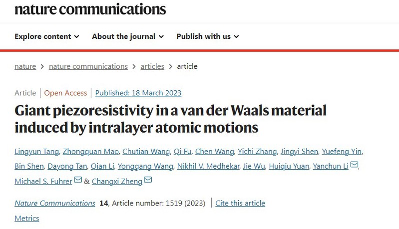
Figure 1 Screenshot of the paper
Van der Waals layered crystals are a class of materials that are coupled only by the weak van der Waals molecular forces between the layers because there is no strong chemical bond in the van der Waals gap. By adjusting the layer spacing, many important physical phenomena can be induced, such as superconductivity, quantum anomalous Hall effect and interlayer exciton condensation. Applying pressure to van der Waals crystals is a very efficient and clean technique for regulating layer spacing. In the past, it was generally believed that the influence of pressure on the physical properties of van der Waals crystals came from two physical mechanisms: anisotropy of lattice contraction and interlayer slip.
The research team found in the pressure experimental study of the layered semiconductor van der Waals crystal β´-In2Se3 that only 1.2Gpa of pressure (pressure) can rapidly reduce the resistivity of this material by 6 orders of magnitude, so that the piezoresistivity of up to -5.33 Gpa-1 can be obtained, which is nearly 25 times higher than the commercial silicon-based piezoresistivity material. This is also the material with the largest piezoresistive coefficient reported among the van der Waals layered crystals (Figure 2). Because β´-In2Se3 layered crystals are very easy to form two-dimensional or quasi-two-dimensional thin film structures by mechanical peeling, β´-In2Se3 is expected to be deeply applied in future robotic and electronic skin.
Figure 2 Paper screenshot: Giant piezoresistive effect of β´-In2Se3
More importantly, the team found a very strong association between the giant piezoresistive effect in β´-In2Se3 and the semiconductor-to-semi-metallic transition that occurs in the crystals under pressure, as well as the loss of linear dichroism (Figure 3). The disappearance of linear dichroism under pressure is an important sign of the movement of Se atoms in the β´-In2Se3 intermediate layer to a high symmetric position. Using first-principles calculations, the team confirmed that the giant piezoresistivity effect of β´-In2Se3 is due to the band gap closure caused by the high symmetric movement of Se atoms in the middle layer within the layer, rather than to the anisotropy of crystal contraction induced by pressure or interlayer slip, which is commonly believed.
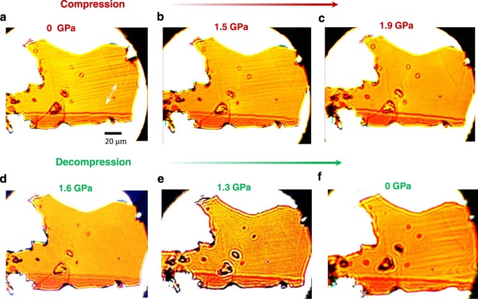
FIG. 3 Screenshot of the paper: Evolution of linear dichroism with pressure
Therefore, the significance of this study is that the research team has not only discovered a van der Waals layered material with excellent piezoresistive properties, but also revealed new degrees of freedom and physical mechanisms to manipulate the electronic structure of van der Waals layered materials.